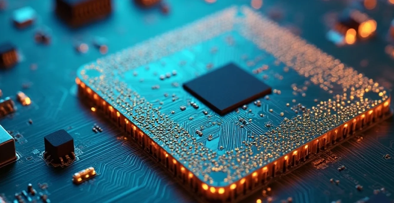
Double-sided printed circuit boards (PCBs) have become an integral component in modern electronics, revolutionizing the way we design and manufacture electronic devices. These versatile boards feature conductive layers on both sides of the substrate, allowing for more complex circuit designs and increased component density. As technology continues to advance, the applications for double-sided PCBs have expanded across various industries, from consumer electronics to military equipment.
The ability to utilize both sides of the board for component placement and routing has opened up new possibilities for miniaturization, improved performance, and enhanced functionality. This technological advancement has enabled engineers and designers to create more sophisticated electronic devices while maintaining compact form factors. Let’s explore the diverse range of applications where double-sided PCBs play a crucial role in shaping our modern technological landscape.
Double-sided PCBs in consumer electronics
Consumer electronics represent one of the most significant sectors utilizing double-sided PCBs. The demand for smaller, more powerful devices has driven the need for efficient circuit board designs that can accommodate complex functionality within limited space. Double-sided PCBs have become the go-to solution for many consumer electronic products, offering a balance between performance and cost-effectiveness.
Compact designs for smartphones and tablets
Smartphones and tablets are prime examples of how double-sided PCBs have enabled remarkable advancements in portable technology. These devices require an intricate network of components to function, including processors, memory chips, wireless modules, and sensors. Double-sided PCBs allow designers to optimize component placement, resulting in thinner and lighter devices without compromising on features or performance.
By utilizing both sides of the board, engineers can create more efficient layouts, reducing signal path lengths and minimizing electromagnetic interference. This approach not only improves the overall performance of smartphones and tablets but also contributes to better battery life and thermal management. The compact nature of double-sided PCBs has been instrumental in the evolution of sleek, powerful mobile devices that we rely on daily.
Enhanced functionality in wearable devices
Wearable technology, such as smartwatches and fitness trackers, has benefited greatly from the adoption of double-sided PCBs. These devices face unique challenges due to their small form factors and the need to incorporate multiple sensors and communication modules. Double-sided PCBs provide the necessary flexibility to pack various components into a confined space while maintaining optimal performance.
The ability to route traces on both sides of the board allows for more efficient interconnections between components, reducing the overall size of the circuit board. This is particularly crucial in wearable devices, where every millimeter counts. Additionally, double-sided PCBs enable better isolation of sensitive analog components from digital circuits, resulting in improved signal integrity and more accurate sensor readings.
Improved performance for gaming consoles
Gaming consoles have become increasingly sophisticated, requiring powerful processors, high-speed memory, and advanced graphics capabilities. Double-sided PCBs play a vital role in meeting these demanding requirements while maintaining a compact form factor. By utilizing both sides of the board, console manufacturers can optimize component placement for better thermal management and signal integrity.
The increased routing options provided by double-sided PCBs allow for more efficient power distribution and signal routing, which is crucial for high-performance gaming systems. This results in faster data processing, reduced latency, and improved overall gaming experience. Furthermore, the ability to incorporate more components on a single board helps reduce the number of interconnects and simplifies the manufacturing process, ultimately leading to more reliable and cost-effective gaming consoles.
Industrial applications of double-sided PCBs
While consumer electronics often grab the spotlight, industrial applications of double-sided PCBs are equally significant. These boards are essential in various industrial sectors, where reliability, durability, and performance are paramount. Let’s explore some key industrial applications that rely heavily on double-sided PCB technology.
Robust designs for automotive electronics
The automotive industry has undergone a significant transformation in recent years, with vehicles becoming increasingly reliant on sophisticated electronic systems. Double-sided PCBs are integral to many automotive applications, from engine control units to advanced driver-assistance systems (ADAS). These boards must withstand harsh operating conditions, including extreme temperatures, vibrations, and electromagnetic interference.
Double-sided PCBs offer several advantages in automotive electronics. The ability to use both sides of the board allows for more compact designs, which is crucial in the space-constrained environment of a vehicle. Additionally, the double-sided PCB for automotive applications provides better thermal management and improved signal integrity, essential for the reliable operation of critical systems. The robust nature of double-sided PCBs also contributes to the longevity and durability of automotive electronic components, ensuring they can withstand the rigors of daily use over many years.
High-reliability solutions for aerospace systems
The aerospace industry demands the highest levels of reliability and performance from electronic components. Double-sided PCBs are widely used in various aerospace applications, including avionics, communication systems, and control panels. These boards must meet stringent requirements for reliability, thermal management, and resistance to environmental factors such as radiation and extreme temperatures.
Double-sided PCBs offer several benefits in aerospace applications:
- Improved signal integrity for critical communication and navigation systems
- Enhanced thermal management capabilities for high-power components
- Reduced weight compared to multilayer boards, contributing to fuel efficiency
- Greater flexibility in component placement and routing for complex systems
- Increased reliability through simplified manufacturing processes
The use of double-sided PCBs in aerospace systems allows engineers to create more compact and efficient designs while meeting the industry’s exacting standards for performance and reliability.
Efficient layouts for industrial control panels
Industrial control panels are the nerve centers of many manufacturing and process control systems. These panels often require a mix of analog and digital circuits, power management components, and communication interfaces. Double-sided PCBs provide an ideal platform for creating efficient and compact control panel layouts.
By utilizing both sides of the board, designers can optimize the placement of components and routing of signals, resulting in several benefits:
- Reduced overall panel size, saving valuable space in industrial environments
- Improved signal isolation between analog and digital circuits
- Enhanced thermal management for power components
- Simplified maintenance and troubleshooting due to cleaner layouts
- Cost-effective solution compared to multilayer boards for many applications
The versatility of double-sided PCBs allows for the creation of modular control panel designs that can be easily customized for different industrial applications, streamlining the development and manufacturing process.
Double-sided PCBs for medical devices
The medical device industry has experienced rapid growth and innovation in recent years, with double-sided PCBs playing a crucial role in enabling advanced diagnostic and therapeutic technologies. These boards are essential components in a wide range of medical devices, from portable patient monitors to sophisticated imaging equipment.
Double-sided PCBs offer several advantages in medical device applications:
- Compact design: Allows for the creation of smaller, more portable medical devices
- Improved signal integrity: Critical for accurate sensor readings and data processing
- Enhanced reliability: Vital for devices that may be life-saving or life-sustaining
- Flexibility in component placement: Enables optimal layouts for complex medical systems
- Cost-effectiveness: Provides a balance between performance and affordability
One of the key areas where double-sided PCBs excel is in wearable medical devices. These devices, such as continuous glucose monitors or ECG patches, require extremely compact and efficient circuit designs. Double-sided PCBs allow engineers to create miniaturized layouts that can accommodate various sensors, processors, and wireless communication modules within a small form factor.
Another significant application is in medical imaging equipment. Double-sided PCBs are used in the signal processing and control systems of devices like ultrasound machines, CT scanners, and MRI equipment. The ability to utilize both sides of the board allows for more efficient routing of high-speed signals and better isolation of sensitive analog components, resulting in improved image quality and system performance.
Double-sided PCBs have revolutionized the design of medical devices, enabling the creation of more compact, reliable, and sophisticated equipment that improves patient care and outcomes.
As medical technology continues to advance, the role of double-sided PCBs in this sector is likely to grow, supporting the development of increasingly sophisticated and patient-friendly medical devices.
Telecommunications equipment using Double-Sided PCBs
The telecommunications industry relies heavily on double-sided PCBs to create efficient and high-performance equipment. From network infrastructure to consumer-grade communication devices, these versatile boards play a crucial role in enabling the rapid transfer of data and voice communications across global networks.
Optimized routing for network switches
Network switches are fundamental components of modern telecommunications infrastructure, responsible for directing data traffic between various devices on a network. Double-sided PCBs are ideal for creating optimized layouts for these complex devices, offering several advantages:
- Improved signal integrity for high-speed data transmission
- Enhanced thermal management for power-hungry components
- Efficient use of space, allowing for higher port densities
- Better isolation between different functional blocks
- Reduced electromagnetic interference (EMI) through strategic component placement
By utilizing both sides of the board, engineers can create more efficient routing paths for high-speed signals, reducing signal degradation and improving overall network performance. The ability to place components on both sides also allows for better thermal management, which is crucial in high-density switch designs where heat dissipation is a significant concern.
High-speed designs for wireless base stations
Wireless base stations form the backbone of cellular networks, handling the transmission and reception of signals between mobile devices and the core network. These stations require sophisticated RF circuits and high-speed digital processing capabilities. Double-sided PCBs provide an excellent platform for designing these complex systems, offering:
- Flexibility in RF component placement for optimal signal performance
- Improved isolation between sensitive RF circuits and digital processing sections
- Enhanced power distribution for high-power amplifiers
- Efficient heat dissipation for thermally challenging components
- Compact designs that reduce the overall size of base station equipment
The use of double-sided PCBs in wireless base stations allows for more efficient and compact designs, which is particularly important as the industry moves towards smaller cell sites and more distributed network architectures in 5G and beyond.
Dense layouts for satellite communication modules
Satellite communication systems require highly specialized and compact electronic modules capable of operating in the harsh environment of space. Double-sided PCBs are often used in these applications due to their ability to create dense, efficient layouts while maintaining the necessary reliability and performance.
Key advantages of using double-sided PCBs in satellite communication modules include:
- Weight reduction, which is critical for space applications
- Improved signal integrity for high-frequency RF circuits
- Enhanced thermal management in the vacuum of space
- Greater flexibility in component placement for optimal performance
- Simplified manufacturing compared to more complex multilayer designs
The ability to create compact and efficient layouts using double-sided PCBs is particularly valuable in satellite applications, where every gram of weight and every millimeter of space counts. These boards enable the development of sophisticated communication payloads that can withstand the rigors of launch and operate reliably in the space environment for extended periods.
Military applications of double-sided PCBs
The military sector has long been at the forefront of technological innovation, and double-sided PCBs play a crucial role in many advanced defense systems. These boards are used in a wide range of military applications, from communication equipment to weapons systems, where reliability, durability, and performance are paramount.
Some key military applications of double-sided PCBs include:
- Tactical radios and secure communication devices
- Guidance systems for missiles and smart munitions
- Electronic warfare and signal intelligence equipment
- Ruggedized computers and displays for field use
- Drone and unmanned vehicle control systems
Double-sided PCBs offer several advantages in military applications:
- Enhanced reliability in harsh environments
- Improved thermal management for high-power components
- Greater flexibility in designing compact, portable equipment
- Better signal integrity for sensitive RF and high-speed digital circuits
- Cost-effective solution for producing specialized military hardware
One of the most critical aspects of military electronics is their ability to withstand extreme conditions. Double-sided PCBs can be designed with special materials and coatings to resist moisture, dust, and chemical exposure. The ability to use both sides of the board also allows for more efficient thermal management, which is crucial for equipment operating in high-temperature environments or with high-power components.
The versatility and reliability of double-sided PCBs make them an ideal choice for many military applications, where failure is not an option and performance must be guaranteed under the most challenging conditions.
As military technology continues to advance, the role of double-sided PCBs is likely to grow. These boards enable the development of increasingly sophisticated and compact electronic systems that provide military forces with critical capabilities in communication, intelligence gathering, and precision engagement.
The use of double-sided PCBs in military applications extends beyond traditional combat systems. They are also utilized in support and logistics equipment, such as inventory management systems, vehicle diagnostics, and maintenance tools. The ability to create robust, portable electronic devices using double-sided PCBs has significantly enhanced the efficiency and effectiveness of military operations across various domains.
Furthermore, the aerospace and defense industry often leads the way in developing new PCB technologies and manufacturing techniques. Innovations in double-sided PCB design and fabrication for military applications often find their way into commercial and industrial products, driving advancements across multiple sectors.