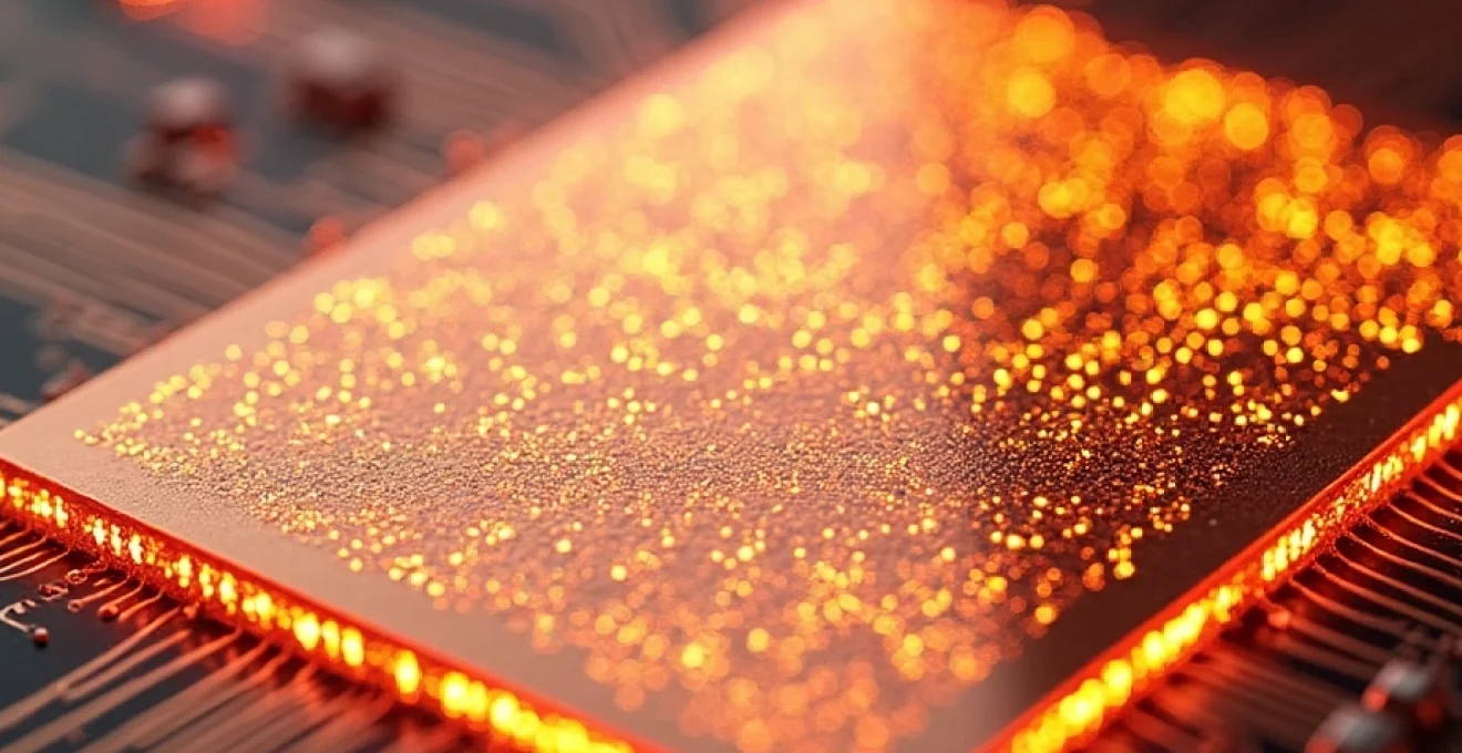
The world of electronics continues to evolve at a rapid pace, with devices becoming more powerful and compact. As a result, the demands placed on printed circuit boards (PCBs) have intensified, particularly in terms of thermal management and electrical performance. Heavy copper PCBs have emerged as a solution to meet these challenges, offering enhanced capabilities that surpass traditional PCB designs. By leveraging the unique properties of copper, these specialized boards are revolutionizing the way engineers approach high-power and high-frequency applications.
Copper PCB advantages for thermal management
One of the primary benefits of heavy copper PCBs is their exceptional thermal management capabilities. As electronic components generate more heat, efficient dissipation becomes crucial for maintaining optimal performance and longevity. Heavy copper PCBs excel in this area, providing several advantages over standard PCB designs.
Enhanced heat dissipation in copper circuits
The increased copper thickness in heavy copper PCBs significantly improves heat dissipation. Copper’s excellent thermal conductivity allows it to efficiently transfer heat away from components, spreading it across the board more evenly. This enhanced heat distribution helps prevent localized hot spots that can lead to component failure or reduced performance. As a result, heavy copper PCBs can handle higher power densities without compromising reliability.
For example, in power electronics applications, where high currents generate substantial heat, heavy copper PCBs can reduce the need for additional cooling mechanisms. This can lead to more compact designs and lower overall system costs. The ICAPE Group offers a range of heavy copper PCB solutions that cater to these demanding thermal requirements.
Improved thermal stability with copper substrates
Heavy copper PCBs also contribute to improved thermal stability in electronic systems. The increased copper mass acts as a heat sink, absorbing and dissipating thermal energy more effectively than thinner copper layers. This thermal buffering effect helps maintain more consistent operating temperatures, reducing thermal stress on components and minimizing the risk of thermal runaway.
Furthermore, the improved thermal stability can lead to better overall system performance. Many electronic components are sensitive to temperature fluctuations, and maintaining a more stable thermal environment can enhance their accuracy and reliability. This is particularly important in precision applications such as instrumentation and measurement devices.
Copper’s high thermal conductivity benefits PCBs
Copper’s inherent high thermal conductivity plays a crucial role in the superior thermal performance of heavy copper PCBs. With a thermal conductivity of approximately 400 W/mK, copper outperforms many other materials commonly used in PCB manufacturing. This property allows heat to spread rapidly across the board, preventing the formation of isolated hot spots.
The benefits of copper’s high thermal conductivity extend beyond just component cooling. It also enables more efficient power distribution across the board, reducing resistive losses and further minimizing heat generation. This synergistic effect contributes to overall improved thermal management and electrical efficiency in heavy copper PCB designs.
Heavy copper PCBs leverage copper’s exceptional thermal conductivity to create a more thermally efficient and stable platform for electronic circuits, enabling higher power densities and improved reliability.
Electrical performance enhancements with copper PCBs
While thermal management is a significant advantage of heavy copper PCBs, their electrical performance benefits are equally impressive. The increased copper thickness and unique properties of copper contribute to several improvements in electrical characteristics, making these PCBs ideal for high-performance applications.
Superior electrical conductivity of copper traces
Copper is renowned for its excellent electrical conductivity, and heavy copper PCBs take full advantage of this property. The thicker copper traces in these boards offer significantly lower resistance compared to standard PCB designs. This reduced resistance translates to several benefits:
- Lower power losses in high-current applications
- Improved efficiency in power distribution networks
- Reduced voltage drops across long traces
- Enhanced current-carrying capacity without overheating
These advantages make heavy copper PCBs particularly well-suited for applications such as power supplies, motor controllers, and high-power LED drivers. The ability to handle higher currents without excessive heating allows for more compact designs and potentially eliminates the need for additional power planes or complex routing schemes.
Reduced signal losses in copper circuits
In addition to improved power handling, heavy copper PCBs also offer benefits for signal integrity. The lower resistance of thicker copper traces results in reduced signal losses, especially at high frequencies. This is particularly important in RF and microwave applications, where maintaining signal strength and minimizing attenuation is crucial.
The reduced signal losses can lead to improved system performance in several ways:
- Extended range in wireless communication systems
- Higher signal-to-noise ratios in sensitive analog circuits
- Improved efficiency in high-frequency power conversion
- Enhanced overall system reliability and performance
Improved signal integrity on copper boards
Heavy copper PCBs also contribute to improved signal integrity through their enhanced impedance control capabilities. The thicker copper layers allow for more precise control of trace impedance, which is critical in high-speed digital and RF applications. This improved impedance control helps minimize signal reflections and distortions, resulting in cleaner signals and reduced electromagnetic interference (EMI).
Furthermore, the increased copper thickness can provide better shielding against external electromagnetic interference, enhancing the overall signal integrity of the system. This is particularly beneficial in noise-sensitive applications or environments with high levels of electromagnetic pollution.
Copper PCB manufacturing considerations
While heavy copper PCBs offer numerous advantages, their manufacturing process requires specialized techniques and considerations. The increased copper thickness presents unique challenges that must be addressed to ensure high-quality, reliable boards.
One of the primary considerations in heavy copper PCB manufacturing is the etching process. The thicker copper layers require longer etching times and more precise control to achieve the desired trace geometries. This can lead to potential issues such as undercutting, where the copper beneath the resist is etched away, resulting in narrower traces than intended.
To address these challenges, manufacturers often employ advanced etching techniques such as differential etching or step etching. These methods allow for better control of the etching process, resulting in more accurate trace widths and improved overall board quality. Additionally, specialized resist materials and exposure techniques may be used to ensure proper adhesion and definition of the copper features.
Another important consideration in heavy copper PCB manufacturing is the lamination process. The increased copper weight can lead to issues with layer registration and overall board flatness. Manufacturers must carefully control the lamination pressure and temperature to ensure proper bonding between layers while maintaining dimensional stability.
Manufacturing heavy copper PCBs requires specialized equipment and expertise to overcome the unique challenges presented by thicker copper layers, ensuring high-quality and reliable boards for demanding applications.
Designing heavy copper PCBs for optimization
Designing heavy copper PCBs requires a different approach compared to standard PCB layouts. Engineers must consider several factors to fully optimize the performance and manufacturability of these specialized boards.
Trace width sizing for current carrying
One of the most critical aspects of heavy copper PCB design is properly sizing trace widths for current-carrying capacity. While the thicker copper allows for higher currents, it’s essential to calculate the appropriate trace width to ensure safe operation without excessive heating. Engineers typically use specialized calculators or design tools that account for factors such as:
- Current requirements
- Copper thickness
- Acceptable temperature rise
- Ambient temperature conditions
- Board thermal characteristics
By accurately sizing traces, designers can maximize the current-carrying capacity of the board while minimizing the risk of overheating or copper delamination. It’s important to note that trace width calculations for heavy copper PCBs may differ from standard IPC guidelines, so using specialized tools or consulting with experienced manufacturers is crucial.
Copper thickness impact on PCB rigidity
The increased copper thickness in heavy copper PCBs has a significant impact on board rigidity. While this can be advantageous in terms of mechanical stability, it also presents challenges in terms of board flexibility and stress management. Designers must carefully consider the copper distribution across the board to avoid issues such as warping or excessive stress on components during thermal cycling.
One approach to managing board rigidity is to strategically vary the copper thickness across different areas of the PCB. This can involve using thicker copper only where high current-carrying capacity is required, while maintaining standard copper thicknesses in other areas. This balanced approach can help optimize both electrical performance and mechanical characteristics.
Thermal via placement for heat dissipation
While heavy copper PCBs offer improved thermal management, strategic placement of thermal vias can further enhance heat dissipation. Thermal vias are plated through-holes that provide a low-resistance path for heat to travel between layers of the PCB. In heavy copper designs, the placement and density of thermal vias can significantly impact overall thermal performance.
When designing thermal via arrays, consider the following factors:
- Via diameter and plating thickness
- Via spacing and pattern
- Proximity to heat-generating components
- Connection to internal plane layers
- Potential impact on signal integrity
By optimizing thermal via placement, designers can create highly efficient heat dissipation pathways that complement the inherent thermal advantages of heavy copper PCBs.
Applications benefiting from heavy copper PCBs
The unique characteristics of heavy copper PCBs make them ideal for a wide range of applications, particularly those involving high power, high frequency, or challenging thermal conditions.
Power electronics leveraging copper’s thermal properties
Power electronics is one of the primary areas where heavy copper PCBs shine. Applications such as motor drives, power inverters, and high-current DC-DC converters benefit greatly from the improved current-carrying capacity and thermal management capabilities of these specialized boards. The ability to handle higher currents without excessive heating allows for more compact designs and potentially eliminates the need for additional cooling mechanisms.
In electric vehicle (EV) applications, heavy copper PCBs are increasingly being used in battery management systems, chargers, and power distribution units. The improved thermal performance helps manage the high currents involved in EV powertrains, contributing to overall system efficiency and reliability.
High-frequency circuits exploiting copper’s conductivity
Heavy copper PCBs also find applications in high-frequency and RF circuits, where signal integrity and low losses are crucial. The reduced resistance of thicker copper traces helps minimize signal attenuation, particularly at higher frequencies. This makes heavy copper PCBs valuable in applications such as:
- Wireless communication systems
- Radar and satellite equipment
- High-speed digital interfaces
- Test and measurement instrumentation
The improved shielding capabilities of heavy copper layers also contribute to better EMI performance, which is critical in many high-frequency applications.
LED applications managing heat with copper
High-power LED lighting is another area where heavy copper PCBs excel. LEDs generate significant heat during operation, and efficient thermal management is crucial for maintaining performance and longevity. Heavy copper PCBs provide an excellent platform for LED arrays, offering superior heat spreading and dissipation compared to standard PCBs.
The improved thermal performance of heavy copper PCBs in LED applications can lead to several benefits:
- Higher LED density without overheating
- Improved color stability and consistency
- Extended LED lifespan
- Reduced need for external heat sinks or cooling mechanisms
These advantages make heavy copper PCBs particularly attractive for high-intensity lighting applications such as stadium lights, automotive headlights, and industrial lighting systems.
As electronic systems continue to push the boundaries of power density and performance, heavy copper PCBs will likely find even more applications across various industries. Their unique combination of thermal management, electrical performance, and reliability makes them an invaluable tool for engineers tackling the challenges of modern electronic design.