Flexible printed circuit boards (flex PCBs) have revolutionized the landscape of modern electronics, enabling unprecedented levels of miniaturization and design flexibility. As consumer devices shrink in size while expanding in functionality, flex PCBs have become indispensable for engineers and manufacturers striving to create smaller, lighter, and more efficient electronic products. Their unique properties allow for innovative form factors and improved performance in a wide range of applications, from smartphones and wearables to medical devices and automotive systems.
Flex PCBs enable smaller electronic device footprints
One of the primary advantages of flex PCBs is their ability to significantly reduce the overall size and weight of electronic devices. This characteristic has become increasingly crucial as consumers demand more compact and portable products. The flexibility of these circuits allows designers to optimize space utilization in ways that were previously impossible with rigid PCBs.
Flexible circuits can be folded into tight spaces
Unlike traditional rigid PCBs, flex circuits can be bent, folded, and shaped to conform to the contours of a device’s housing. This malleability allows engineers to utilize spaces that would otherwise be wasted, effectively increasing the functional density of the product. For example, a flex PCB can be folded around corners or curved surfaces, eliminating the need for multiple boards connected by cables or connectors.
The ability to fold flex PCBs into tight spaces is particularly valuable in devices with complex internal geometries. Smartphones, for instance, leverage this property to pack an impressive array of components into an incredibly slim profile. By using flex PCBs, designers can route circuits through narrow gaps and around obstacles, maximizing the use of every available millimeter within the device.
Flex PCBs reduce overall device size and weight
The inherent thinness of flex PCBs contributes significantly to weight reduction in electronic devices. Compared to rigid PCBs, flex circuits can be up to 75% lighter and occupy up to 10 times less space. This dramatic reduction in weight and volume allows manufacturers to create products that are not only more portable but also more energy-efficient, as less power is required to operate lighter components.
Moreover, the use of flex PCBs often eliminates the need for bulky connectors and cables, further reducing the overall size and weight of the device. This streamlined design approach not only contributes to a sleeker product appearance but also enhances reliability by reducing the number of potential failure points in the system.
Compact flexible designs ideal for portable electronics
The compact nature of flex PCB designs makes them ideal for portable electronic devices where space is at a premium. Wearable technology, such as smartwatches and fitness trackers, benefits tremendously from the use of flex PCBs. These devices must pack a multitude of sensors, processors, and communication modules into a form factor that is comfortable to wear and aesthetically pleasing.
Similarly, flex PCB solutions for industrial electronics have enabled the development of ultra-thin laptops, tablets, and e-readers that offer enhanced functionality without compromising on portability. The flexibility of these circuits allows for innovative designs that were previously unattainable, such as foldable smartphones and rollable displays.
Enhanced reliability and durability with flex circuits
While the space-saving properties of flex PCBs are impressive, their contribution to device reliability and durability is equally significant. The unique characteristics of flexible circuits make them particularly well-suited for applications that require resistance to environmental stresses and mechanical strain.
Flexible substrates withstand vibration and physical stress
One of the key advantages of flex PCBs is their ability to withstand vibration and physical stress better than their rigid counterparts. The flexible substrate material, typically polyimide, can absorb and distribute mechanical forces more effectively than rigid materials. This property is particularly valuable in applications such as automotive electronics, aerospace systems, and industrial machinery, where components are subjected to constant vibration and shock.
In these demanding environments, flex PCBs can maintain electrical connectivity and performance even under severe conditions. Their ability to flex and bend with applied forces reduces the risk of solder joint fatigue and component failure, leading to increased product longevity and reliability.
Polyimide material provides excellent thermal stability
The polyimide material commonly used in flex PCBs offers exceptional thermal stability, allowing these circuits to operate reliably across a wide temperature range. This characteristic is crucial for electronic devices that may be exposed to extreme temperatures, such as those found in automotive under-hood applications or outdoor telecommunication equipment.
Polyimide can withstand temperatures from -65°C to 125°C without significant degradation of its electrical or mechanical properties. This thermal resilience ensures that flex PCBs maintain their performance and structural integrity even in challenging thermal environments, contributing to the overall reliability of the electronic system.
Flex PCBs resist breakage from repeated flexing
Unlike rigid PCBs, which can crack or break when subjected to repeated bending, flex PCBs are designed to withstand thousands of flex cycles without failure. This property is essential for applications where the circuit must undergo frequent bending or folding during normal operation, such as in foldable smartphones or laptop hinges.
The ability to resist breakage from repeated flexing not only enhances the durability of the device but also opens up new possibilities for product design. Engineers can create movable or articulating parts within electronic devices without worrying about the premature failure of the circuitry due to mechanical stress.
Streamlined assembly process using flexible circuit boards
Flex PCBs offer significant advantages in the manufacturing and assembly process of electronic devices. Their unique properties allow for more efficient production methods and can lead to substantial cost savings in high-volume manufacturing scenarios.
One of the primary benefits of using flex PCBs is the reduction in the number of interconnections required within a device. Traditional rigid PCB designs often necessitate multiple boards connected by cables or connectors, each representing a potential point of failure and adding complexity to the assembly process. Flex PCBs, on the other hand, can be designed as a single, continuous circuit that spans multiple planes within the device, eliminating the need for many of these connections.
This streamlined approach to circuit design translates into fewer assembly steps, reduced labor costs, and a lower risk of assembly errors. For example, in smartphone manufacturing, a single flex PCB can replace several rigid boards and connecting cables, simplifying the production process and improving overall product reliability.
The use of flex PCBs can reduce assembly time by up to 50% and lower production costs by as much as 30% compared to traditional rigid PCB designs.
Furthermore, the flexibility of these circuits allows for easier installation in tight or irregularly shaped spaces. Assemblers can manipulate the PCB to fit around obstacles or conform to curved surfaces, reducing the need for complex mounting hardware or custom-shaped rigid boards. This adaptability not only speeds up the assembly process but also contributes to the overall space efficiency of the final product.
Flex PCBs facilitate High-Density interconnect designs
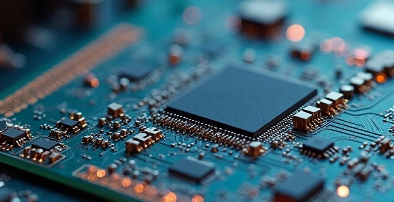
As electronic devices become more sophisticated, the demand for high-density interconnect (HDI) designs has increased dramatically. Flex PCBs are particularly well-suited to meet this challenge, offering several advantages over traditional rigid PCBs in achieving higher component densities and more complex routing schemes.
Fine-pitch traces allow dense component placement
Flex PCBs enable the creation of extremely fine-pitch traces, allowing for denser component placement and more intricate circuit designs. The flexible substrate material and advanced manufacturing techniques permit the creation of traces and spaces as small as 25 microns (0.001 inches). This level of precision is difficult to achieve consistently with rigid PCBs, especially in high-volume production.
The ability to create such fine features allows designers to pack more components into a smaller area, directly contributing to the miniaturization of electronic devices. For instance, in the design of modern smartphones, this capability is crucial for fitting all the necessary components, including multiple cameras, sensors, and antennas, into an increasingly slim form factor.
Multilayer flex circuits enable complex routing schemes
Flex PCBs can be manufactured with multiple layers, similar to rigid PCBs, but with the added benefit of flexibility. These multilayer flex circuits allow for complex routing schemes that would be challenging or impossible to achieve with rigid boards alone. Designers can create three-dimensional circuit paths, routing signals through different layers and directions to optimize signal integrity and minimize electromagnetic interference.
This capability is particularly valuable in applications requiring high-speed data transmission or where signal integrity is critical. By carefully designing the layer stack-up and utilizing controlled impedance techniques, engineers can ensure optimal performance even in densely packed circuits.
HDI flexible boards minimize interconnect lengths
High-density interconnect (HDI) flex PCBs offer the advantage of minimizing interconnect lengths between components. Shorter trace lengths result in reduced signal propagation delays, lower power consumption, and improved overall system performance. This is especially crucial in high-frequency applications where every millimeter of trace length can impact signal quality.
By allowing components to be placed closer together and utilizing advanced via technologies such as microvia and buried vias, HDI flex PCBs enable the creation of extremely compact and efficient circuit designs. This level of integration is essential for cutting-edge technologies like 5G communication systems and advanced driver assistance systems (ADAS) in automotive applications.
Flexible circuits improve signal integrity performance
Signal integrity is a critical concern in modern electronic design, particularly as data rates continue to increase and devices become more compact. Flex PCBs offer several advantages in maintaining signal integrity, making them an attractive option for high-speed and high-frequency applications.
One of the key benefits of flex PCBs in terms of signal integrity is their ability to maintain consistent impedance throughout the circuit. The tightly controlled manufacturing process for flex circuits allows for precise control of trace width, spacing, and dielectric thickness, resulting in more predictable and uniform impedance characteristics. This consistency is crucial for minimizing signal reflections and ensuring clean signal transmission in high-speed digital circuits.
Additionally, the flexibility of these circuits allows for optimized routing paths that can reduce signal skew and crosstalk. Designers can create smooth, curved traces that minimize abrupt changes in direction, which can cause signal reflections and degradation. This capability is particularly valuable in differential pair routing, where maintaining consistent spacing and length matching is critical for signal integrity.
Flex PCBs can support data rates exceeding 25 Gbps, making them suitable for the most demanding high-speed applications in telecommunications and data center environments.
Another advantage of flex PCBs in signal integrity performance is their inherent ability to reduce electromagnetic interference (EMI). The thin profile of flex circuits and their ability to be shaped and routed to avoid potential sources of interference can significantly reduce EMI issues within a device. This characteristic is particularly valuable in densely packed electronic products where multiple high-frequency components must coexist without interfering with each other.
Furthermore, the use of flex PCBs can enable better thermal management, which indirectly impacts signal integrity. By allowing for more efficient heat dissipation through optimized component placement and the use of thermal management features like copper planes, flex PCBs can help maintain stable operating temperatures. This temperature stability is crucial for maintaining consistent electrical characteristics and ensuring reliable signal transmission over time.